
Preparation and characterization of copper doped titanium dioxide thin film by sparking process
Keywords:
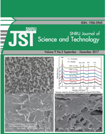
Cu-doped TiO2, thin films, nanoparticles, sparking processAbstract
The advantages of copper (Cu) doping into Titanium Dioxide (TiO2) semiconductor could reduce the band gap energy of TiO2 and enhance visible light absorption. Pure and Cu-doped TiO2 nanoparticles thin films of about 900 – 1200 nm thickness were successfully deposited onto glass substrates by sparking process. To obtain a uniformfilm thickness, the substrate was moved rotate around an area of 1 × 1 cm2. The films were annealed at 500 °C for 60 min. The doping ratios of Cu-doped TiO2 were 2, 7, 12, 18 and 23 atomic%. The effects of dopants content on optical properties were investigated. Scanning electron spectroscopy (SEM) images indicated agglomerated particle size decrease with increasing the Cu content after annealing treatment, and energy dispersive X-ray spectroscopy (EDS) analysis confirm contents of copper into TiO2. Raman spectra reveal the annealed samples at 500 °C are anatase combined with rutile phase. Ultraviolet-visible (UV-Vis) spectroscopy study is used to characterize the effect of copper dopant with different concentrations on the band gap energies of TiO2 nanoparticles. The absorbance spectra
indicated increase visible region and the band gap energy decreased with increasing copper contents
Downloads
Published
2017-10-30
How to Cite
Tipparak, P. (2017). Preparation and characterization of copper doped titanium dioxide thin film by sparking process. Creative Science, 9(3), 583–591. retrieved from https://ph01.tci-thaijo.org/index.php/snru_journal/article/view/102448
Issue
Section
Research Article