
Effects of sputtering pressure on the growth of AlGaN thin films using Co-sputtering technique
DOI:
https://doi.org/10.55674/ias.v13i1.251506Keywords:
AlGaN, Co-sputtering, Room temperature, RFMS, HiPIMSAbstract
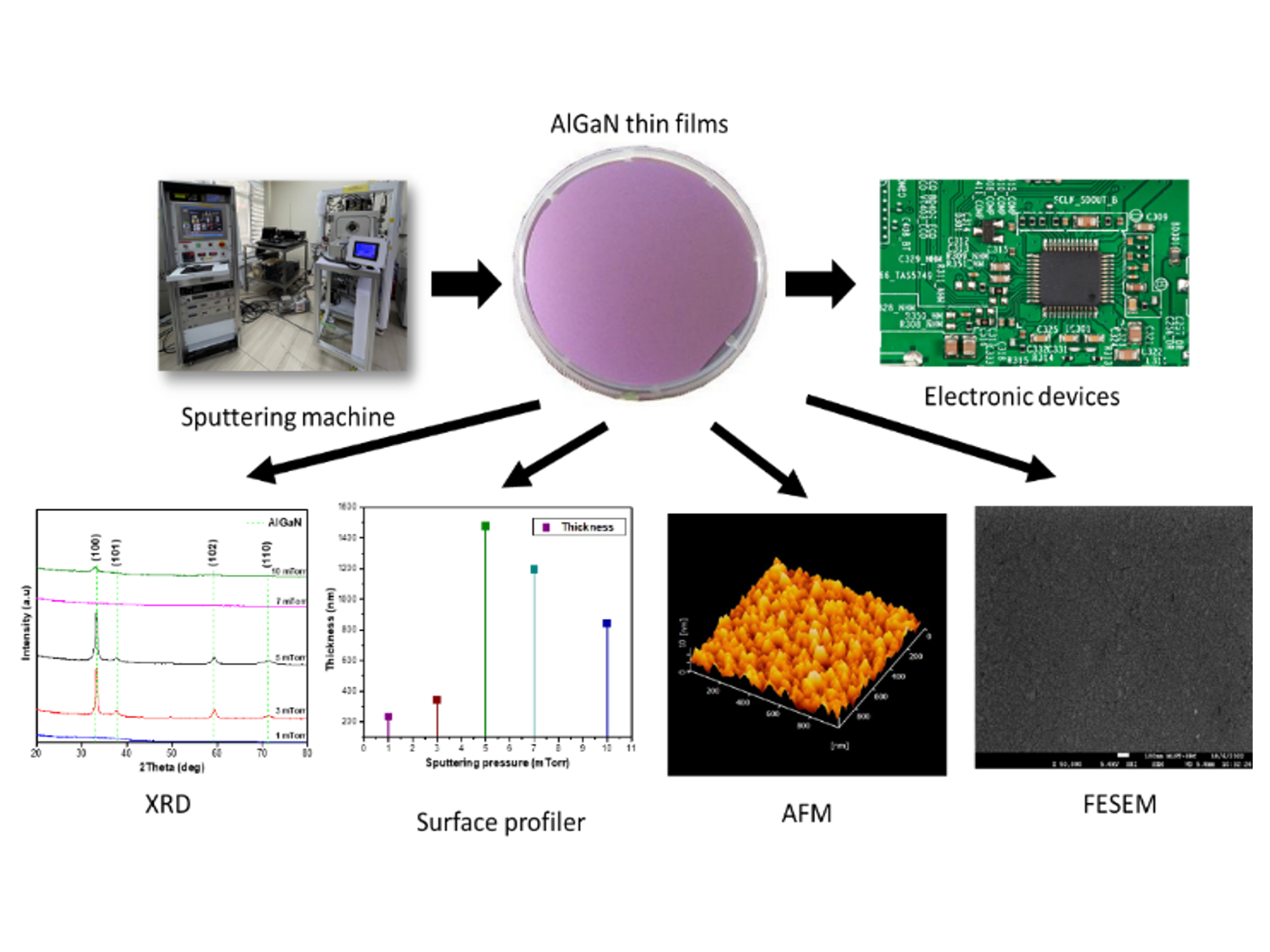
Aluminium gallium nitride (AlGaN) thin films provide promise for a variety of electronic devices due to their wide energy bandgap, which ranges from 3.11 – 6.40 eV. Here, a co-sputtering approach utilising the RF and HiPIMS power supply of magnetron sputtering is used to deposit the AlGaN thin films. To examine their impact on the structural characteristics and morphology of the thin films, the AlGaN thin films were deposited under various sputtering pressures using the co-sputtering technique. Following that, the films were examined using X-ray diffraction (XRD), atomic force microscopy (AFM), field emission scanning electron microscopy (FESEM), and surface profiling to determine their characteristics. XRD shows the polycrystalline AlGaN with (100), (101), (102), and (110) plane for the AlGaN deposited at a sputtering pressure of 3 mTorr and 5 mTorr with FWHM 0.622° and 0.732°, respectively. The increasing the sputtering pressure to 5 mTorr is found to improve the crystallinity as well as the thickness of the AlGaN thin films from 234.27 – 1479.37 nm. AFM examination of the AlGaN film revealed a trend of increasing roughness and grain size together up to 3.25 nm and 47.22 nm respectively, with rising sputtering pressure from 1 – 7 mTorr. The co-sputtering of AlGaN can be successfully demonstrated in this study, and it is also shown that the sputtering pressure has a substantial impact on the development of AlGaN thin films produced using this technology.
References
Q. Hua, B. Ma, and W. Hu, Aluminum, Gallium, and Indium Nitrides, Encyclopedia of Material: Science and Technology. 3 (2021) 1 – 10.
Y. Li, W. Wang, Y. Lin, X. Li, L. Huang, Y. Zheng, Z. Zhang, G. Li, Growth of high-quality AlGaN epitaxial films on Si substrates. Materials Letters, 207 (2017), 133 – 136.
A. Jarndal, AlGaN/GaN HEMTs on SiC and Si substrates: A review from the small-signal-modeling’s perspective, Int. J. RF Microw. Comput. Eng. 24(3) (2014) 389 – 400.
S. Kang, U. Chatterjee, D. Y. Um, I. S. Seo, C. R. Lee, Growth and characterization of n-AlGaN 1-D structures with varying Al composition using u-GaN seeds, J. Cryst. Growth. 480 (2017) 108 – 114.
Y. Cordier, Gallium Nitride (GaN): Physics, Devices, and Technology, CRC Press. (2017) 45–61.
H. Xin Jing, C.A. Che Abdullah, M.Z. Mohd Yusoff, A. Mahyuddin, Z. Hassan, Structural and optical properties of AlN/GaN and AlN/AlGaN/GaN thin films on silicon substrate prepared by plasma assisted molecular beam epitaxy (MBE), Results Phys. 12 (2019) 1177 – 1181.
S. Choi, A.S. Ansari, H.J. Yun, H. Kim, B. Shong,
B.J. Choi, Growth of Al-rich AlGaN thin films by purely thermal atomic layer deposition, J. Alloys Compd. 854 (2021) 157186.
X.Y. Liu , S.X. Zhao, L.Q. Zhang, H.F. Huang, J.S. Shi, C.M. Zhang, D.W. Zhang, AlGaN/GaN MISHEMTs with AlN gate dielectric grown by thermal ALD technique, Nanoscale Res. Lett. 10(1) (2015) 1 – 6.
A.H. Simon, Handbook of Thin Film Deposition, Fourth Edition, Applied Science, (2018) 195 – 230.
A. Mantarci, Role of RF power in growth and characterization of RF magnetron sputtering GaN/glass thin film, Emerg. Mater. Res. 8(3) (2019) 320 – 330.
A. Mantarcı, M. Kundakçi, Physical properties of RF magnetron sputtered GaN/n-Si thin film: impacts of RF power, Opt. Quantum Electron. 51(3) (2019) 81.
D.L. Ma , H.Y. Liu, Q.Y. Deng, W.M. Yang, K. Silins, N. Huang, Y.X. Leng, Optimal target sputtering mode for aluminum nitride thin film deposition by high power pulsed magnetron sputtering, Vacuum, 160 (5) (2019) 410 – 417.
S. Lin, J. Zhang, R. Zhu, S. Fu, D. Yun, Effects of sputtering pressure on microstructure and mechanical properties of ZrN films deposited by magnetron sputtering, Mater. Res. Bull. 105(5) (2018) 231 – 236.
L. Li, T. Xue, Z. Song, C. Liu, F. Ma, Effect of sputtering pressure on surface roughness, oxygen vacancy and electrical properties of a-IGZO thin films, Xiyou Jinshu Cailiao Yu Gongcheng/Rare Met. Mater. Eng. 45 (8) (2016) 1992 – 1996.
X. Zhang, X.H. Song, D.L. Zhang, Thickness dependence of grain size and surface roughness for dc magnetron sputtered Au films, Chinese Phys. B. 19(8) (2010) 6 – 10.
V. Perumal , U. Hashim, SC. Gopinath, R. Haarindraprasad, W. W. Liu, P. Poopalan, A.R. Ruslinda, Thickness dependent nanostructural, Morphological, Optical and impedometric analyses of zinc oxide-Gold hybrids: Nanoparticle to thin film, PLoS One. 10 (12) (2015) 1 – 24.
A. Safdar, H.Z. He, L.Y. Wei, A. Snis, L.E. Chavez De Paz, Effect of process parameters settings and thickness on surface roughness of EBM produced Ti-6Al-4V, Rapid Prototyp. J. 18(5) (2012) 401 – 408.
S. Mobtakeri, Y. Akaltun, A. Özer, M. Kılıç, E.Ş. Tüzemen, E. Gür, Gallium oxide films deposition by RF magnetron sputtering; a detailed analysis on the effects of deposition pressure and sputtering power and annealing, Ceram. Int. 47 (2) (2021) 1721 – 1727.
M. Ohtsuka, H. Takeuchi, H. Fukuyama, Effect of sputtering pressure on crystalline quality and residual stress of AlN films deposited at 823K on nitrided sapphire substrates by pulsed DC reactive sputtering, Jpn. J. Appl. Phys. 55(5) (2016).
Downloads
Published
How to Cite
Issue
Section
License
Copyright (c) 2024 J. Mater. Sci. Appl. Energy

This work is licensed under a Creative Commons Attribution-NonCommercial-NoDerivatives 4.0 International License.