
A study of annealing temperatures on electrical conductivity and optical properties of nanostructure ITO film as deposited by ion assisted e-beam evaporation
DOI:
https://doi.org/10.55674/ias.v11i2.244615Keywords:
Nanostructured ITO, Anneal treatment, Ion assisted E-Beam evaporationAbstract
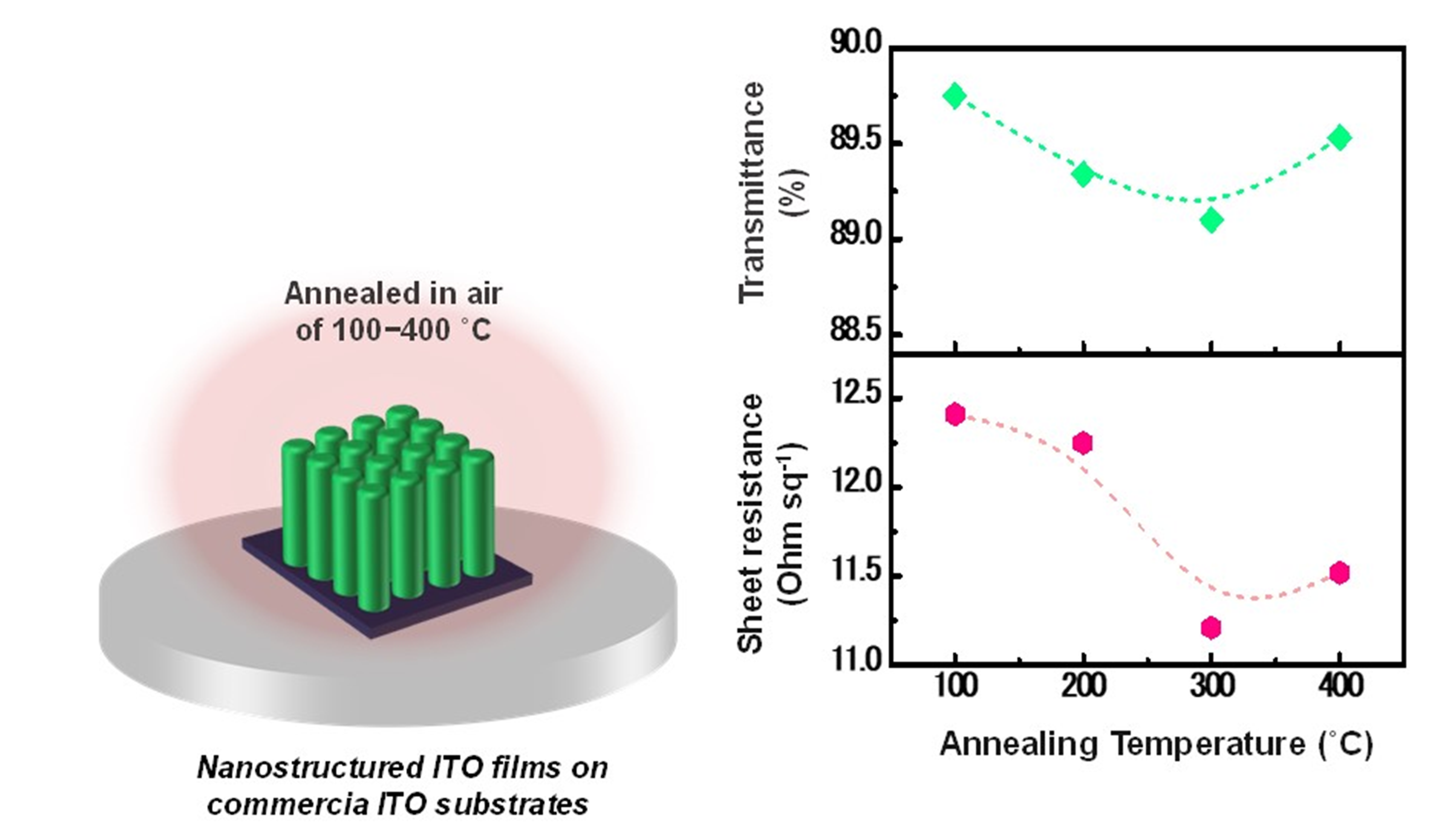
In this research, the electrical and optical properties of nanostructured Indium Tin Oxide (ITO) films were investigated. The ITO films were deposited by ion assisted e-beam evaporation with the glancing angle deposition (GLAD) technique on commercial ITO substrates, followed by annealing treatment. The results of crystal structure showed that the nanostructured ITO films are polycrystalline and cubic bixbyite structure (222). The sheet resistance and average transmission at the visible region were 12.17 W sq−1 and 89 %, respectively. The films presented the lowest resistivity and good transparency, where the sheet resistance and an average transmittance were 11.21 W sq−1 and 91% after annealing. The omnidirectional characteristics for a wide range of incident angle (0 − 80°) of nanostructured ITO film which was annealed at 300 °C had higher optical transmission than films without annealing. This work eventually proved that the plasma treatments have effectively promoted the performance of the dye-sensitized solar cells and confirmed their potentials in the real-world applications.
References
J. Du, X. liang Chen, C. chi Liu, J. Ni, G. fu Hou, Y. Zhao, X. dan Zhang, Highly transparent and conductive indium tin oxide thin films for solar cells grown by reactive thermal evaporation at low temperature, Appl. Phys. A Mater. Sci. Process. 117 (2014) 815 – 822.
A. Valla, P. Carroy, F. Ozanne, D. Muñoz, Understanding the role of mobility of ITO films for silicon heterojunction solar cell applications, Sol. Energy Mater. Sol. Cells. 157 (2016) 874 – 880.
S.K. Park, J.I. Han, W.K. Kim, M.G. Kwak, Deposition of indium-tin-oxide films on polymer substrates for application in plastic-based flat panel displays, Thin Solid Films. 397 (2001) 49 – 55.
J. Hotovy, J. Hüpkes, W. Böttler, E. Marins, L. Spiess, T. Kups, V. Smirnov, I. Hotovy, J. Kováč, Sputtered ITO for application in thin-film silicon solar cells: Relationship between structural and electrical properties, Appl. Surf. Sci. 269 (2013) 81 – 87.
Y. Gil, H. Kim, Hybrid ITO transparent conductive electrodes embedded with Pt nanoclusters for enhanced output efficiency of GaN-based light-emitting diodes, Thin Solid Films. 603 (2016) 307 – 312.
W. Wang, H. Peng, S. Chen, Highly transparent quantum-dot light-emitting diodes with sputtered indium-tin-oxide electrodes, J. Mater. Chem. C. 4 (2016) 1838 – 1841.
C.J.M. Emmott, A. Urbina, J. Nelson, Environmental and economic assessment of ITO-free electrodes for organic solar cells, Sol. Energy Mater. Sol. Cells. 97 (2012) 14 – 21.
Y.S. Park, E. Kim, B. Hong, J. Lee, Characteristics of ITO films with oxygen plasma treatment for thin film solar cell applications, Mater. Res. Bull. 48 (2013) 5115 – 5120.
M. Ismail, A.M. Rana, I. Talib, T.L. Tsai, U. Chand, E. Ahmed, M.Y. Nadeem, A. Aziz, N.A. Shah,
M. Hussain, Room-temperature fabricated, fully transparent resistive memory based on ITO/CeO2/ITO structure for RRAM applications, Solid State Commun. 202 (2015) 28 – 34.
S. Xu, Y. Shi, Low temperature high sensor response nano gas sensor using ITO nanofibers, Sens. Actuators B Chem. 143 (2009) 71 – 75.
X. Li, G.M. Kale, Influence of thickness of ITO sensing electrode film on sensing performance of planar mixed potential CO sensor, Sens. Actuators B Chem. 120 (2006) 150 – 155.
P. Nuchuay, T. Chaikeeree, M. Horprathum, N. Mungkung, N. Kasayapanand, C. Oros, S. Limwichean, N. Nuntawong, C. Chananonnawathorn, V. Patthanasettakul, P. Muthitamongkol, B. Samransuksamer, S. Denchitcharoen, A. Klamchuen, C. Thanachayanont, P. Eiamchai, Engineered omnidirectional antireflection ITO nanorod films with super hydrophobic surface via glancing-angle ion-assisted electron-beam evaporation deposition, Curr. Appl. Phys. 17 (2017) 222 – 229.
D.P. Pham, B.T. Phan, V.D. Hoang, H.T. Nguyen, T.K.H. Ta, S. Maenosono, C.V. Tran, Control of preferred (222) crystalline orientation of sputtered indium tin oxide thin films, Thin Solid Films. 570 (2014) 16 – 19.
P. Canhola, N. Martins, L. Raniero, S. Pereira, E. Fortunato, I. Ferreira, R. Martins, Role of annealing environment on the performances of large area ITO films produced by rf magnetron sputtering, Thin Solid Films. 487 (2005) 271 – 276.
N.M. Ahmed, F.A. Sabah, H.I. Abdulgafour, A. Alsadig, A. Sulieman, M. Alkhoaryef, The effect of post annealing temperature on grain size of indium-tin-oxide for optical and electrical properties improvement, Results Phys. 13 (2019) 102159.
N. Manavizadeh, A. Khodayari, E. Asl Soleimani, S. Bagherzadeh, M.H. Maleki, Structural properties of post annealed ITO thin films at different temperatures, Iran. J. Chem. Chem. Eng. 28 (2009) 57 – 61.
Downloads
Published
How to Cite
Issue
Section
License
Copyright (c) 2022 Journal of Materials Science and Applied Energy

This work is licensed under a Creative Commons Attribution-NonCommercial-NoDerivatives 4.0 International License.