The Deposition Times of Teflon Thin Films by PECVD Technique Affecting to Peel-off of PDMS Molding in Micro-Nano Structure for Surface Enhanced Raman Spectroscopy

Authors

  • Wantana Koetniyom Department of Industrial Physics and Medical Instrumentation, Faculty of Applied Science, King Mongkut’s University of Technology North Bangkok, Bangsue, Bangkok, 10800 Thailand
  • Pacharamon Somboonsaksri Department of Industrial Physics and Medical Instrumentation, Faculty of Applied Science, King Mongkut’s University of Technology North Bangkok, Bangsue, Bangkok, 10800 Thailand
  • Sukon Kalasung National Electronics and Computer Technology Center, National Science and Technology Development Agency, Khlong Luang, Pathum Thani, 12120 Thailand
  • Chanunthorn Chananonnawathorn National Electronics and Computer Technology Center, National Science and Technology Development Agency, Khlong Luang, Pathum Thani, 12120 Thailand
  • Viyapol Patthanasettakul National Electronics and Computer Technology Center, National Science and Technology Development Agency, Khlong Luang, Pathum Thani, 12120 Thailand
  • Mati Horprathum National Electronics and Computer Technology Center, National Science and Technology Development Agency, Khlong Luang, Pathum Thani, 12120 Thailand
  • Pitak Eiamchai National Electronics and Computer Technology Center, National Science and Technology Development Agency, Khlong Luang, Pathum Thani, 12120 Thailand
  • Noppadon Nuntawong National Electronics and Computer Technology Center, National Science and Technology Development Agency, Khlong Luang, Pathum Thani, 12120 Thailand
  • Saksorn Limwichean National Electronics and Computer Technology Center, National Science and Technology Development Agency, Khlong Luang, Pathum Thani, 12120 Thailand

Keywords:

Teflon, PECVD Technique, PDMS Molding, SERs applications

Abstract

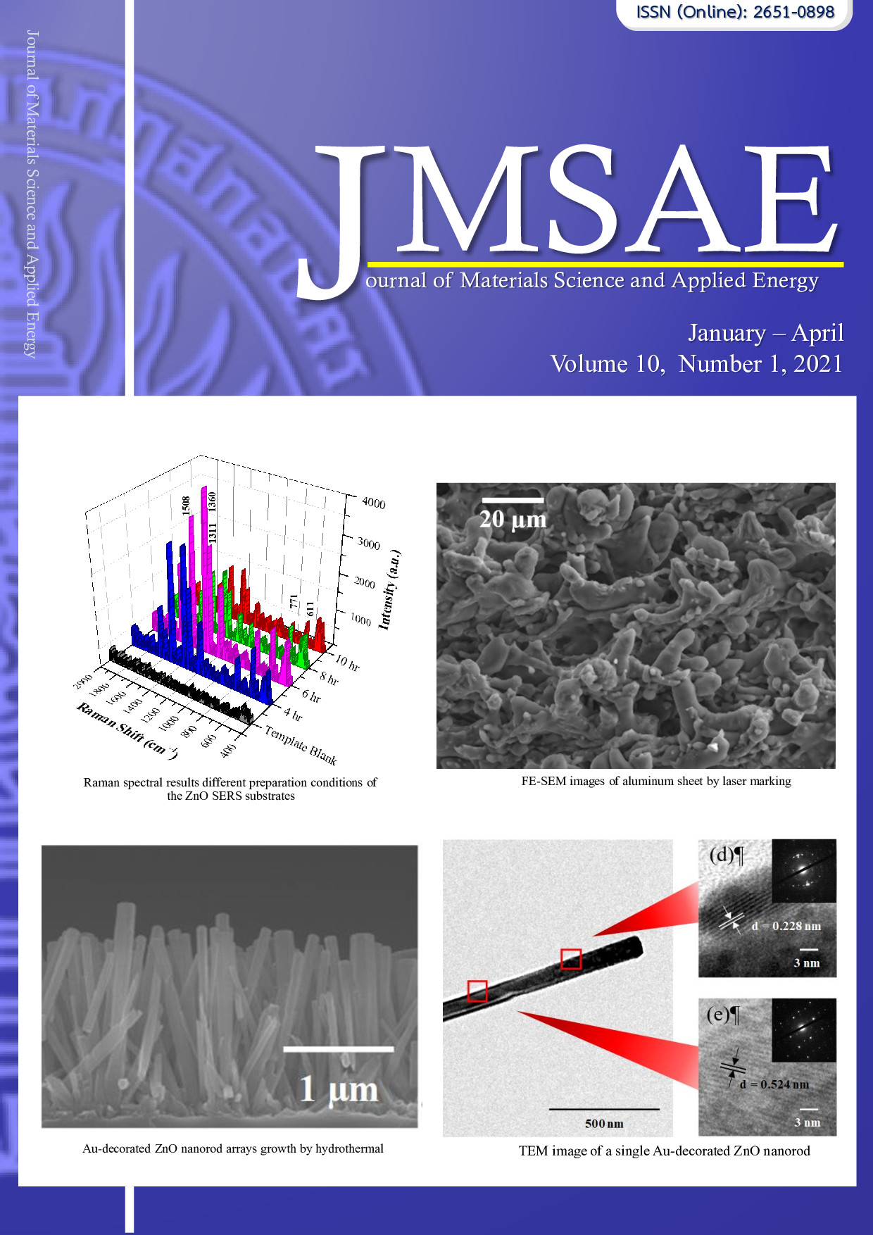
In this research, we have studied the thickness of Polytetrafluoroethylene (PTFE) or Teflon thin films layer on Nano-in-Micro structure scale by Plasma Enhanced Chemical Vapor Deposition (PECVD) technique. Especially, the deposition time are various at 5 - 20 min and tested manually Teflon peeling-off from PDMS template for SERs applications. After tested peeling-off, a magnetron sputtering system is used to decorate the PDMS molding with silver nanoparticles for 180 s. The PDMS template was investigated by Field-emission Scanning Electron Microscopy (FE-SEM) and Raman Spectroscopy. The PDMS template was observed the hydrophobic properties by contact angle measurement. The result indicated that the thickness of the Teflon film layer related with the number of peeling-off from the PDMS template which can be observed from the intensity of Raman signal by testing with Rhodamine 6G (R6G) concentration of 1 ´ 10-5 M. FE-SEM result showed the thickness of Teflon films was increased from 50.78 ‒ 210.37 nm. in accordance with deposition time. The contact angle indicated that Teflon can easily help to peel-off PDMS template than un-coating. The optimum deposit time is 20 min and can peel-off of PDMS template into 5 cycles that can be observed by Raman intensity is remaining stable.

Downloads

Published

2020-12-31

How to Cite

Koetniyom, W., Somboonsaksri, P., Kalasung, S., Chananonnawathorn, C., Patthanasettakul, V., Horprathum, M. ., Eiamchai, P., Nuntawong, N., & Limwichean, S. (2020). The Deposition Times of Teflon Thin Films by PECVD Technique Affecting to Peel-off of PDMS Molding in Micro-Nano Structure for Surface Enhanced Raman Spectroscopy. Journal of Materials Science and Applied Energy, 10(1), 1–8. Retrieved from https://ph01.tci-thaijo.org/index.php/jmsae_ceae/article/view/241036